
Auger Electron Spectroscopy
David Mogk, Imaging and Chemical Analysis Laboratory, Montana State University
What is Auger Electron Spectroscopy
Auger Electron Spectroscopy (AES) is a surface-sensitive analytical method the provides compositional information in the near-surface environment of materials (typically 1-5 atomic monolayers, 3-10 nm depth). AES is widely used in materials sciences, although it has not been widely used in the Earth and Environmental Sciences (see references below). AES has been applied to study of a wide variety of surface-mediated reactions such as sorption, catalysis, REDOX, photolytic, and dissolution/precipitation reactions, and the formation of thin films and coatings on materials. AES is capable of detecting all elements except for H and He. Because AES uses a focused elelctdron beam, sub-micron mapping of distribution of elements on material surfaces is possible. Quantitative analysis of surface composition is possible using published elemental sensitivity factors or by comparison with standards. Coupled with a sputter gun, chemical stratigraphy on an atomic scale can be obtained by depth profiling methods. AES is a powerful technique that provides information that is complementary to other surface methods such as X-ray Photoelectron Spectroscopy (XPS) and Time of Flight Secondary Ion Mass Spectrometry (ToF-SIMS), and "bulk" analytical methods such as electron probe microanalysis (EPMA) and X-ray Fluorescence (XRF) methods.
Fundamental Principles of Auger Electron Spectroscopy
Electron-Sample Interactions result in a number of responses such as secondary and back-scattered electrons and secondary X-rays that are widely used to image and obtain chemical information about materials. The presence of the Auger electron is often ignored (or unknown) in geoscience applications. The Auger electron has a very low energy and is readily sorbed by the surrounding material matrix. Thus, if an Auger electron is detected, it must have escaped from the near-surface environment of the top few atomic monolayers (3-50 nm).

![[reuse info]](/images/information_16.png)

The "Auger effect" was discovered simultaneously in 1922 by Pierre Auger and Lise Meitner (although the history of science has largely ignored her contribution). When an inner shell electron of an atom is ejected in response to an excitation source (typically a high energy electron beam in AES, but impinging X-rays also produce this effect--Auger lines can be observed in X-ray photoelectron spectroscopy, XPS ,data), an outer shell electron must drop to the core level. This produces a secondary X-ray of wavelength fixed by the difference in energies between the orbitals, or ejection of a secondary electron, the Auger electron. For instance, the ejection of a K-shell electron often results in drop of one electron from the L-shell electron to the core level and ejection of the second Auger electron from the L-shell. Thus, this is referred to as the KLL transition. The energy of the Auger electron is measured as kinetic energy as eV. The Auger electron has an energy given by: EAuger = EK– EL1 – EL2,3 - f where EK, EL1and EL2,3 are the binding energies of the K1, L1 and L2,3 electron orbits of the atom and f is the work function. Production of Auger electrons is very efficient for light elements compared with secondary X-rays for corresponding elements; this sensitivity for detection of light elements is one of the strengths of AES analysis. Auger electrons have relatively small intensities compared with their background, so it may be difficult to resolve these peaks in an acquired spectrum. Consequently, it has become customary to show the differentiated spectrum to facilitate identifying and measuring peak positions.


![[creative commons]](/images/creativecommons_16.png)

Auger Electron Spectroscopy Instrumentation - How Does It Work?

An AES instrument is basically an advanced SEM that also includes a) an ultrahigh vacuum system, b) Auger electron spectrometer, and c) ion sputter gun. Critical components include:
- Ultrahigh vacuum system (UHV). Typically, AES instruments are operate at pressures <10-9torr. This is important because 1) gas in the sample chamber can impede (i.e. absorb) the transfer of Auger electrons from the material surface to the detector, so UHV optimizes counting efficiency; and 2) material surfaces tend to be highly reactive so UHV is needed to prevent contamination through sorption of gases on the material surface.
- Electron source. AES uses a focused electron beam to stimulate the material surface, and thus standard SEM images are obtained. These images provide a spatial maps of structures or textures that can define regions of interest for targeted AES analysis. Modern AES instruments typically use a Field Emission electron source which allows spatial resolution down to ~ 5 nanometers.

- Electron Energy Analyzer. A big breakthrough in the development of AES is the use of the Cylindrical Mirror Analyzer (CMA). This detector has proven to have a high collection efficiency and good energy resolution.
- Ion Gun. The ion gun uses a focused beam of ionized gas (usually Ar) at the sample to clean off surface (often called adventitious) contaminants. As the AES comes from only a few atomic monolayers at a material surface, any sorbed gases will be detected on a material "as received" that has been in contact with the atmosphere. A rastered area is defined to "dust off" any surface contaminants, and this area is usually on the scale of mm x mm which is significantly larger than the region of interest for analysis. The ion gun is also used to produce depth profilesacross surfaces to document compositional changes across material interfaces. The sputter rate can be calibrated by using oxide-coated metal standards to determine sputter rates in terms of nm/second depending on the accelerating potential of the ion gun and the cross-sectional area of the ion beam. In some cases, the ablation pit formed under the ion beam can be directly measured using an atomic force microscope. The ion beam may actually implant some surface components into the bulk material in a "knock on" effect that may complicate analysis of surface components and their depth on/in materials.

- Other Detectors. As the AES instrument is basically a Field Emission SEM, it is possible to add other detectors on the instrument. The PHI 710 AES instrument at the Imaging and Chemical Analysis Laboratory, Montana State University is uniquely equipped with additional EDS and EBSD detectors. This means that analyses can be done in situ on micron-scale particles in near real-time to acquire: 1) high resolution SEM images (FESEM), 2) bulk compositional data and elemental mapping. (EDS), and 3) phase identification based on electron diffraction and crystallographic orientation data (EBSD). This instrument is shown below.

Applications
AES is widely used in numerous types of material science. Typical applications include:
- Analysis of thin films and coatings
- When combined with ion sputtering, elemental depth profiles reveal information on the thicknesses of coatings and the nature of interfacial layers.
- Identification of particulate matter, dopants or contaminants.
- Studies of corrosion
Of interest to geoscientists, is the use of AES to analyze a number of different types of surface-mediated reactions:
- Sorption
- Catalysis
- Dissolution/precipitation
- REDOX and photolytic reactions
Strengths and Limitations of Auger Electron Spectroscopy?
Strengths

- AES is a surface-sensitive spectroscopy with detection limits of ~0.1 at%.
- The top few atomic monolayers are analyzed (0.4-10 nm), and there are very few matrix effects.
- When run in survey mode, inventories of all surface components can be obtained for any element of Z≥3 (Li and heavier). Light element analysis is a particular strength of AES.
- Maps of the distribution of elements on material surfaces can be obtained on the sub-micron scale. This is very useful for determining the compositional homogeneity or heterogeneity of material surfaces.
- Depth profiles are obtained using an ion sputter gun to determine the thicknesses of surface layers on a material substrate. The ability to obtain nanometer-scale chemical stratigraphy is an important way to monitor changes in process and physico-chemical conditions imposed on materials.
- A Multiplex modecan be used to monitor specific energy windows in the Auger spectrum that is associated with a given element of interest. This is commonly used in conjunction with the ion sputter gun to monitor changes in abundances of selected elements as a function of depth.
- Semi-quantitative analyses are obtained by applying published Auger sensitivity factors, or be comparing with standards.
Limitations
Limitations in using AES include:
- Samples must be compatible with an ultrahigh vacuum environment. Samples that are volatile or that are unstable under an electron beam should not be analyzed (e.g., epoxies, organic compounds).
- Surface contamination is almost always present, and some preliminary sputtering of the surface is usually required (e.g., removal of adventitious carbon).
- Standardization of the composition of material surfaces is difficult. Use of the sensitivity factors to obtain relative compositions is useful, but in detail must be viewed as a semi-quantitative analysis.
- The biggest drawback of AES is that it has proven difficult to analyze insulating samples (i.e., minerals!). A conducting coat, as used in other SEM or EMPA methods, cannot be used as AES would only be able to analyze the applied conducting coat. However, recent advances in charge compensation methods has reduced this limitation. In addition, creative sample preparation methods can also help minimize local charging problems: a) use very small samples that are mounted on an indium substrate (In is both conducting and malleable, so samples can be easily embedded), b) mount the specimen on a conducting Si wafer and attach with a very small dab of conducting colloidal graphite paint, c) mask a small region of interest, and then apply a standard C or Au coat and analyze near the edges of the masked area, d) place a fine Cu grid over the insulating sample but be aware that the height of the grid may be in the way of transfer of Auger electrons to the detector, and e) operate at a low beam voltage (1-3 keV), but these conditions will not permit collection of EDS X-ray elemental data if there is a need to compare surface and bulk compositions.
User's Guide - Sample Collection and Preparation
Sample preparation: In general, AES analyzes samples "as received". Any treatments applied to the sample will most likely introduce contaminants and alter the surface composition. Small samples (less than a few mm's) are preferred to minimize outgassing and charging problems. Flat samples are also preferred to minimize charging, and also to produce better surface elemental maps. As described above, numerous methods may need to be used to minimize charging problems on insulating samples.
Data Collection, Results and Presentation
These are examples of the type of mapping and spectroscopic data that can be obtained using AES. These results are from recent studies of corrosion of carbon steel in the vicinity of MnS inclusions.
- Avci, R., Davis, B.H., Rieders, N., Lucas, K., Nandasiri, M. and Mogk, D., 2018. Role of Metallurgy in the Localized Corrosion of Carbon Steel. Journal of Minerals and Materials Characterization and Engineering, 6(6), pp.618-646.
- Rieders, N., Nandasiri, M., Mogk, D. and Avci, R., 2021. New Insights into Sulfide Inclusions in 1018 Carbon Steels. Metals, 11(3), p.428.
The gray image in the upper left is a SEM image of a corrosion pit that developed around a MnS inclusion. The yellow box shows the area of interest used for the collection of an EDS spectrum on the inclusion (blue spectrum) and AES analysis of the inclusion (red spectrum, upper right). Note that the EDS spectrum does not show the presence of Cu, but Cu is evident as a surface component in the AES spectrum. Cu occurs as a thin coating on this inclusion (nm scale) but is transparent to the EDS signal as this derives from the excitation volume that is 1-3 microns deep. It is often the case that surface AES analyses are very different than the underlying "bulk" analyses obtained by EDS. The series of colored elemental AES maps show the host steel (Fe) and MnS inclusion with Cu coating. The Si rich area is a contaminant particle from the Si-colloid polishing procedure that was used.

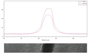
The following two images show a) an AES depth profile across the MnS inclusion, showing a 4 nm thick oxidized layer that also contains the Cu coating; and b) an AES linescan across the MnS inclusion.

The following images are from an AES study of chemically weathered hornblende, showing a) a depth profile that demonstrates incongruent dissolution of the hornblende, with different components released from different depths in the hornblende, and b) a series of AES spectra obtained at different depths on the hornblende after different periods of sputtering with the ion gun. After Mogk, D.W. and Locke III, W.W., 1988. Application of auger electron spectroscopy (AES) to naturally weathered hornblende. Geochimica et Cosmochimica Acta, 52(10), pp.2537-2542.


Literature
The following literature can be used to further explore Auger Electron Spectroscopy
Theory and Practice of Auger Electron Spectroscopy
- Baer, D.R., Lea, A.S., Geller, J.D., Hammond, J.S., Kover, L., Powell, C.J., Seah, M.P., Suzuki, M., Watts, J.F. and Wolstenholme, J., 2010. Approaches to analyzing insulators with Auger electron spectroscopy: Update and overview. Journal of Electron Spectroscopy and Related Phenomena, 176(1-3), pp.80-94.
- D. Briggs and M. P. Seah, Practical Surface Analysis by Auger and X-ray Photoelectron Spectroscopy, John Wiley and Sons, New York, 1983.
- Powell, C.J. and Seah, M.P., 1990. Precision, accuracy, and uncertainty in quantitative surface analyses by Auger‐electron spectroscopy and x‐ray photoelectron spectroscopy. Journal of Vacuum Science & Technology A: Vacuum, Surfaces, and Films, 8(2), pp.735-763.
- Powell, C.J., Jablonski, A., Werner, W.S. and Smekal, W., 2005. Characterization of thin films on the nanometer scale by Auger electron spectroscopy and X-ray photoelectron spectroscopy. Applied Surface Science, 239(3-4), pp.470-480.
- Prutton, M., 2006, Scanning Auger Electron Microscopy, Wiley, 368 p.
Applications of Auger Electron Spectroscopy Applied to Earth and Environmental Science
- Bakken, B.M., Hochella, M.F., Marshall, A.F. and Turner, A.M., 1989. High-resolution microscopy of gold in unoxidized ore from the Carlin mine, Nevada. Economic Geology, 84(1), pp.171-179.
- Browning, R. and Hochella Jr, M.F., 1990. Auger electron spectroscopy and microscopy. In Instrumental Analysis of Geological Materials (pp. 87-120). VCH Publishers Inc.
- Floss, C. and Stadermann, F., 2009. Auger Nanoprobe analysis of presolar ferromagnesian silicate grains from primitive CR chondrites QUE 99177 and MET 00426. Geochimica et Cosmochimica Acta, 73(8), pp.2415-2440.
- Hochella, M.F., Harris, D.W. and Turner, A.M., 1986. Scanning Auger microscopy as a high-resolution microprobe for geologic materials. American Mineralogist, 71(9-10), pp.1247-1257.
- Hochella Jr, M.F., Turner, A.M. and Harris, D.W., 1986. High resolution scanning Auger microscopy of mineral surfaces. Scanning Electron Microscopy, 1986(2), p.2.
- Hochella, M.F., 1988. Auger electron and X-ray photoelectron spectroscopies. Spectroscopic Methods in Mineralogy and Geology,Reviews in Mineralogy, volume 18, chapter 13, pp.573-638.
- Hochella Jr, M.F., Ponader, H.B., Turner, A.M. and Harris, D.W., 1988. The complexity of mineral dissolution as viewed by high resolution scanning Auger microscopy: Labradorite under hydrothermal conditions. Geochimica et Cosmochimica Acta, 52(2), pp.385-394.
- Hochella Jr, M.F. and Brown Jr, G.E., 1988. Aspects of silicate surface and bulk structure analysis using X-ray photoelectron spectroscopy (XPS). Geochimica et Cosmochimica Acta, 52(6), pp.1641-1648.
- Hyland, M.M., Jean, G.E. and Bancroft, G.M., 1990. XPS and AES studies of Hg (II) sorption and desorption reactions on sulphide minerals. Geochimica et Cosmochimica Acta, 54(7), pp.1957-1967
- Junta, J.L. and Hochella Jr, M.F., 1994. Manganese (II) oxidation at mineral surfaces: A microscopic and spectroscopic study. Geochimica et Cosmochimica Acta, 58(22), pp.4985-4999.spectroscopic evidence for sorption and reduction. Geochimica et Cosmochimica Acta, 58(13), pp.2829-2843.
- Mackinnon, I.D. and Mogk, D.W., 1985. Surface sulfur measurements on stratospheric particles. Geophysical research letters, 12(2), pp.93-96.
- Mogk, D.W. and Locke III, W.W., 1988. Application of auger electron spectroscopy (AES) to naturally weathered hornblende. Geochimica et Cosmochimica Acta, 52(10), pp.2537-2542.
- Mogk, D.W., 1990. Application of Auger electron spectroscopy to studies of chemical weathering. Reviews of Geophysics, 28(4), pp.337-356.
- Mycroft, J.R., Nesbitt, H.W. and Pratt, A.R., 1995. X-ray photoelectron and Auger electron spectroscopy of air-oxidized pyrrhotite: Distribution of oxidized species with depth. Geochimica et Cosmochimica Acta, 59(4), pp.721-733.
- Nesbitt, H.W. and Pratt, A.R., 1995. Applications of Auger-electron spectroscopy to geochemistry. The Canadian Mineralogist, 33(2), pp.243-259.
- Pratt, A.R., Muir, I.J. and Nesbitt, H.W., 1994. X-ray photoelectron and Auger electron spectroscopic studies of pyrrhotite and mechanism of air oxidation. Geochimica et Cosmochimica Acta, 58(2), pp.827-841.
- Stadermann, F.J., Floss, C., Bose, M. and Lea, A.S., 2009. The use of Auger spectroscopy for the in situ elemental characterization of sub‐micrometer presolar grains. Meteoritics & Planetary Science, 44(7), pp.1033-1049.
- Stipp, S.L., Hochella Jr, M.F., Parks, G.A. and Leckie, J.O., 1992. Cd2+ uptake by calcite, solid-state diffusion, and the formation of solid-solution: Interface processes observed with near-surface sensitive techniques (XPS, LEED, and AES). Geochimica et Cosmochimica Acta, 56(5), pp.1941-1954.
- Vollmer, C., Hoppe, P., Stadermann, F.J., Floss, C. and Brenker, F.E., 2009. NanoSIMS analysis and Auger electron spectroscopy of silicate and oxide stardust from the carbonaceous chondrite Acfer 094. Geochimica et Cosmochimica Acta, 73(23), pp.7127-7149.
- Wersin, P., Hochella Jr, M.F., Persson, P., Redden, G., Leckie, J.O. and Harris, D.W., 1994. Interaction between aqueous uranium (VI) and sulfide minerals: spectroscopic evidence for sorption and reduction. Geochimica et Cosmochimica Acta, 58(13), pp.2829-2843.
Related Links
For more information about Auger Electron Spectroscopy follow the links below.
Teaching Activities and Resources
Teaching activities, labs, and resources pertaining to Auger Electron Spectroscopy.
An instructional Powerpoint slideshow on Auger Electron Spectroscopy Overview (PowerPoint 2007 (.pptx) 4.7MB May7 21) has been made available by PHI Electronics.


