Scanning Electron Microscopy (SEM)
Susan Swapp, University of Wyoming
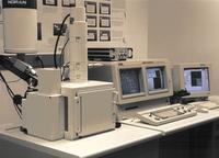
What is Scanning Electron Microscopy (SEM)
×
Fundamental Principles of Scanning Electron Microscopy (SEM)
Accelerated electrons in an SEM carry significant amounts of kinetic energy, and this energy is dissipated as a variety of signals produced by electron-sample interactions when the incident electrons are decelerated in the solid sample. These signals include secondary electrons (that produce SEM images), backscattered electrons (BSE), diffracted backscattered electrons (EBSD that are used to determine crystal structures and orientations of minerals), photons (characteristic X-rays that are used for elemental analysis and continuum X-rays), visible light (cathodoluminescence--CL), and heat. Secondary electrons and backscattered electrons are commonly used for imaging samples: secondary electrons are most valuable for showing morphology and topography on samples and backscattered electrons are most valuable for illustrating contrasts in composition in multiphase samples (i.e. for rapid phase discrimination). X-ray generation is produced by inelastic collisions of the incident electrons with electrons in discrete ortitals (shells) of atoms in the sample. As the excited electrons return to lower energy states, they yield X-rays that are of a fixed wavelength (that is related to the difference in energy levels of electrons in different shells for a given element). Thus, characteristic X-rays are produced for each element in a mineral that is "excited" by the electron beam. SEM analysis is considered to be "non-destructive"; that is, x-rays generated by electron interactions do not lead to volume loss of the sample, so it is possible to analyze the same materials repeatedly.
Scanning Electron Microscopy (SEM) Instrumentation - How Does It Work?

×
- Electron Source ("Gun")
- Electron Lenses
- Sample Stage
- Detectors for all signals of interest
- Display / Data output devices
- Infrastructure Requirements:
- Power Supply
- Vacuum System
- Cooling system
- Vibration-free floor
- Room free of ambient magnetic and electric fields
Applications

×
Strengths and Limitations of Scanning Electron Microscopy (SEM)?
Strengths
There is arguably no other instrument with the breadth of applications in the study of solid materials that compares with the SEM. The SEM is critical in all fields that require characterization of solid materials. While this contribution is most concerned with geological applications, it is important to note that these applications are a very small subset of the scientific and industrial applications that exist for this instrumentation. Most SEM's are comparatively easy to operate, with user-friendly "intuitive" interfaces. Many applications require minimal sample preparation. For many applications, data acquisition is rapid (less than 5 minutes/image for SEI, BSE, spot EDS analyses.) Modern SEMs generate data in digital formats, which are highly portable.
Limitations
Samples must be solid and they must fit into the microscope chamber. Maximum size in horizontal dimensions is usually on the order of 10 cm, vertical dimensions are generally much more limited and rarely exceed 40 mm. For most instruments samples must be stable in a vacuum on the order of 10-5 - 10-6 torr. Samples likely to outgas at low pressures (rocks saturated with hydrocarbons, "wet" samples such as coal, organic materials or swelling clays, and samples likely to decrepitate at low pressure) are unsuitable for examination in conventional SEM's. However, "low vacuum" and "environmental" SEMs also exist, and many of these types of samples can be successfully examined in these specialized instruments. EDS detectors on SEM's cannot detect very light elements (H, He, and Li), and many instruments cannot detect elements with atomic numbers less than 11 (Na). Most SEMs use a solid state x-ray detector (EDS), and while these detectors are very fast and easy to utilize, they have relatively poor energy resolution and sensitivity to elements present in low abundances when compared to wavelength dispersive x-ray detectors (WDS) on most electron probe microanalyzers (EPMA). An electrically conductive coating must be applied to electrically insulating samples for study in conventional SEM's, unless the instrument is capable of operation in a low vacuum mode.
User's Guide - Sample Collection and Preparation
Sample preparation can be minimal or elaborate for SEM analysis, depending on the nature of the samples and the data required. Minimal preparation includes acquisition of a sample that will fit into the SEM chamber and some accommodation to prevent charge build-up on electrically insulating samples. Most electrically insulating samples are coated with a thin layer of conducting material, commonly carbon, gold, or some other metal or alloy. The choice of material for conductive coatings depends on the data to be acquired: carbon is most desirable if elemental analysis is a priority, while metal coatings are most effective for high resolution electron imaging applications. Alternatively, an electrically insulating sample can be examined without a conductive coating in an instrument capable of "low vacuum" operation.
Data Collection, Results and Presentation
Representative SEM images of asbestiform minerals from the USGS Denver Microbeam Laboratory
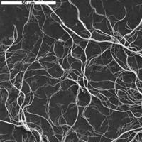 UICC Asbestos Chrysotile 'A' standard
 Tremolite asbestos, Death Valley, California
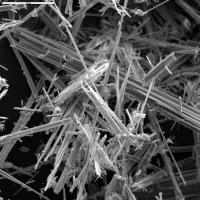 Anthophyllite asbestos, Georgia
 Winchite-richterite asbestos, Libby, Montana

×

×

×

×
Literature
The following literature can be used to further explore Scanning Electron Microscopy (SEM)
- Goldstein, J. (2003) Scanning electron microscopy and x-ray microanalysis. Kluwer Adacemic/Plenum Pulbishers, 689 p.
- Reimer, L. (1998) Scanning electron microscopy : physics of image formation and microanalysis. Springer, 527 p.
- Egerton, R. F. (2005) Physical principles of electron microscopy : an introduction to TEM, SEM, and AEM. Springer, 202.
- Clarke, A. R. (2002) Microscopy techniques for materials science. CRC Press (electronic resource)
Related Links
For more information about Scanning Electron Microscopy (SEM) follow the links below.
- Petroglyph--An atlas of images using electron microscope, backscattered electron images, element maps, energy dispersive x-ray spectra, and petrographic microscope -- Eric Chrisensen, Brigham Young University
- SEM/EDX webpage from Indiana University - Purdue University Fort Wayne
Teaching Activities and Resources
Teaching activities, labs, and resources pertaining to Scanning Electron Microscopy (SEM).
- Argast, Anne and Tennis, Clarence F., III, 2004, A web resource for the study of alkali feldspars and perthitic textures using light microscopy, scanning electron microscopy and energy dispersive X-ray spectroscopy, Journal of Geoscience Education 52, no. 3, p. 213-217.
- Beane, Rachel, 2004, Using the Scanning Electron Microscope for Discovery Based Learning in Undergraduate Courses, Journal of Geoscience Education, vol 52 #3, p. 250-253
- Moecher, David, 2004, Characterization and Identification of Mineral Unknowns: A Mineralogy Term Project, Jour. Geoscience Education, v 52 #1, p. 5-9.


