
Wavelength-Dispersive X-Ray Spectroscopy (WDS)
When an electron beam of sufficient energy interacts with a sample target it generates X-rays, as well as derivative electrons (e.g. secondary, back-scattered, auger). A wavelength-dispersive spectrometer uses the characteristic X-rays generated by individual elements to enable quantitative analyses (down to trace element levels) to be measured at spot sizes as small as a few micrometers. WDS can also be used to create element X-ray compositional maps over a broader area by means of rastering the beam. Together, these capabilities provide fundamental quantitative compositional information for a wide variety of solid materials. This technique is complementary to energy-dispersive spectroscopy (EDS) in that WDS spectrometers have significantly higher spectral resolution and enhanced quantitative potential. Many SEM and EPMA instruments have EDS systems mounted to the column, and an EPMA typically has an array of several WDS spectrometers for simultaneous measurement of multiple elements. In typical EPMA applications, EDS is used for quick elemental scans to find out what a material contains, and WDS is then used to acquire precise chemical analyses of selected phases.
How it Works - WDS
A wavelength-dispersive (WD) spectrometer is used to isolate the X-rays of interest for quantitative analysis. There may be a single WD spectrometer horizontally mounted on an electron column (more typical in SEM instruments) or 4-5 spectrometers may be mounted vertically in sequence around the sample chamber (more typical of EPMA).
WDS analysis involves four steps that must work together to achieve optimal results.
- A beam of electrons is accelerated in an evacuated electron column of an EPMA or SEM to the sample surface with sufficient energy (typically with a potential difference of 15-20 kV) to generate characteristic X-rays for the elements to be analyzed.
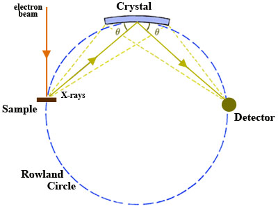
- Once X-rays are generated in the sample, they are selected using an analytical crystal(s) with specific lattice spacing(s). The geometry of the X-ray generating sample and the analytical crystal is such that they maintain a constant take-off angle. When X-rays encounter the analytical crystal at a specific angle Θ, only those X-rays that satisfy Bragg's Law are reflected and a single wavelength is passed on to the detector. The wavelength of the X-rays reflected into the detector may be varied by changing the position of the analyzing crystal relative to the sample i.e. the X-ray source-crystal distance is a linear function of the wavelength. Consequently, X-rays from only one element at a time can be measured on the spectrometer and the position of a given analytical crystal must be changed in order to adjust to a wavelength characteristic of another element. There are two types of analytical geometry currently in use. The first type, the Johann geometry, is constructed by bending the analytical crystal to a radius of 2R, where R is the radius of the focusing circle, the Rowland circle (Fig. 1). The second type, the Johansson geometry, is bent to a radius 2R and then ground to radius R, so that all of points of reflection lie on the Rowland circle, which maximizes the collection efficiency of the spectrometer. There is commonly more than a single analytical crystal in a WD spectrometer and, in the case of most EPMA instruments, there are typically multiple spectrometers with a suite of analytical crystals. Several different analytical crystals with dissimilar crystal lattice spacings (d-spacings) are normally used for WDS so that the spectrometers can reach all of the elemental wavelengths of interest and it will optimize performance in different wavelength ranges. An EPMA configured with 5 spectrometers, for example, might be set up to run WDS in a sequence to acquire 10 elements from one unknown sample by cycling through each crystal during analysis.
- X-rays of specific wavelengths from the analytical crystal are passed on to the X-ray detector. The sample, crystal, and detector must lie on the Rowland circle and remain on it for all wavelengths of interest in order to focus X-rays efficiently. Because the sample and take-off angle of the X-rays are fixed, the analytical crystal and detector must both move to remain on the Rowland circle. In addition, the analytical crystal rotates as the X-ray source-crystal distance changes (requiring clever and precise engineering!). Detectors used in WD spectrometers are most commonly gas proportional counter types, in which incoming X-rays enter the detector through a collimator (slit) and thin window, are absorbed by atoms of the counter gas, and then a photoelectron is ejected by each atom absorbing an X-ray. The photoelectrons are accelerated to a central wire such that additional ionization produces an electrical pulse which has an amplitude proportional to the energy of the original X-ray photon. The two general types of detector use sealed and gas-flow proportional counters. The sealed proportional counters are typically used for high-energy X-ray lines and have a relatively thick window (~50 ???m thick Be window) that prevents leakage of Xe or Xe-CO2 gas in the detector. The gas-flow proportional counters typically are used for low-energy lines, have ultrathin windows (0.5-1 ???m mylar or polypropylene windows), and use a counter gas (generally P-10; Ar gas with 10% methane) that flows through the detector at a constant rate.
- Within a given sample, once the x-ray intensities of each element of interest are "counted" in a detector at a specific beam current, the count rates are compared to those of standards containing known values of the elements of interest. In turn, the x-ray intensities must be corrected for matrix effects associated with atomic number (Z), absorption (A) and fluorescence (F). This correction procedure is performed within a computer program that takes the raw counting rates of each element, compares these to standards, computes the ZAF correction (or similar type of correction) and displays the results as a function of the weight % of the oxides or elements.
Thus, measurement of an element's abundance requires exciting an atom to produce X-rays, focusing the X-rays through a crystal spectrometer to a detector, converting the X-rays to photoelectrons, which in turn generate an electrical signal whose magnitude is proportional to the abundance of the element! This multi-step process involves many potential breakdowns, but works reliably well to allow for routine analysis.
Strengths
- WDS is used for non-destructive quantitative analyses of spots as small as a few micrometers, at detection levels as low as a few 10s of ppmw, and for elements from atomic number 5 (boron) and higher.
- WDS works well in a variety of natural and synthetic solid materials, including minerals, glasses, tooth enamel, semi-conductors, ceramics, metals, etc.
- The high spatial resolution of WDS not only allows quantitative analyses to be performed on small phases but also to detect chemical zoning on a small scale within a material (e.g. mineral).
- When the electron beam is rastered, the WD spectrometers can allow x-ray image maps of individual elements to be constructed.
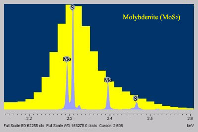
- When compared to EDS, WDS exhibits superior peak resolution of elements (Fig. 2) and sensitivity of trace elements (Fig. 3).


Limitations
- Because WDS cannot determine elements below atomic number 5 (boron), several geologically important elements cannot be measured with WDS (e.g., H, Li, and Be).
- Despite the improved spectral resolution of elemental peaks, some peaks exhibit significant overlaps that result in analytical challenges (e.g., VKα and TiKβ).
- WDS analyses are not able to distinguish among the valence states of elements (e.g. Fe2+ vs. Fe3+) such that this information must be obtained by other techniques (e.g. Mossbauer spectroscopy).
- The multiple masses of an element (i.e. isotopes) cannot be determined by WDS, but rather are most commonly obtained with a mass spectrometer (see stable and radiogenic isotope techniques).
Results
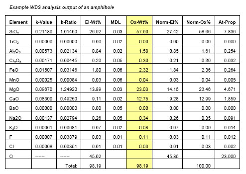
WDS can result in high resolution wavelength spectra (e.g. Figs. 2,3) and high quality element x-ray compositional maps, but the most common application of WDS is for quantitative spot analysis. Typically, individual WDS spot analyses include information on the ratio of the WDS detector counts of the sample relative to the counts on a standard for each element (k-Ratio), a measure of the minimum detection limits of an element (MDL), the weight % of each element (El-Wt%), the weight % of each element expressed as an oxide (Ox-Wt%) that results after the matrix correction is made and the atomic proportions (At-Prop) based on a fixed oxygen normalization basis (Table 1). The El-Wt% or Ox-Wt% are typically used as input for a subsequent calculation of the stoichiometry of a mineral or material that is most appropriate to the nature of the material. This stoichiometric calculation is generally based on a fixed number of oxygens or cations or metals depending on the sample being analyzed.
Mineral formulae calculation programs can be found in the Teaching Phase Equilibria module; these include spreadsheet programs and related on-line resources for calculating the structural formulae for most rock-forming minerals.
References
- Goldstein, J. (2003) Scanning electron microscopy and x-ray microanalysis. Kluwer Adacemic/Plenum Pulbishers, 689 p.
- Reimer, L. (1998) Scanning electron microscopy : physics of image formation and microanalysis. Springer, 527 p.
- Egerton, R. F. (2005) Physical principles of electron microscopy : an introduction to TEM, SEM, and AEM. Springer, 202.
- Clarke, A. R. (2002) Microscopy techniques for materials science. CRC Press (electronic resource)