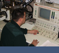
Electron Backscatter Diffraction (EBSD)
What is EBSD?
Accelerated electrons in the primary beam of a scanning electron microscope (SEM) can be diffracted by atomic layers in crystalline materials. These diffracted electrons can be detected when they impinge on a phosphor screen and generate visible lines, called Kikuchi bands, or "EBSP's" (electron backscatter patterns). These patterns are effectively projections of the geometry of the lattice planes in the crystal, and they give direct information about the crystalline structure and crystallographic orientation of the grain from which they originate. When used in conjunction with a data base that includes crystallographic structure information for phases of interest and with software for processing the EPSP's and indexing the lines, the data can be used to identify phases based on crystal structure and also to perform fabric analyses on polycrystalline aggregates.
How does EBSD work?
The polished sample is placed in the SEM and inclined approximately 70o relative to normal incidence of the electron beam. The detector is actually a camera equipped with a phosphor screen integrated with a digital frame grabber. The camera resides on a horizontally mounted motorized carriage. It is inserted to within several mm of the surface of the inclined sample. The optimal arrangement results when the camera is as close to the sample as possible while avoiding the possibility of collision between the sample surface and the delicate phosphor screen. The pattern of Kikuchi lines on the phosphor screen is electronically digitized and processed to recognize the individual Kikuchi lines. These data are used to identify the phase, to index the pattern, and to determine the orientation of the crystal from which the pattern was generated. [insert ebsp_index.jpg here - improve this later with a picture of a crystal showing orientation below the indexed pattern] Individual mineral grains can be selected for identification and determination of crystal orientation, or data may be acquired on a grid over a selected area of the surface of the sample to determine the identity, orientations, and spatial relations between a large number of grains. These data can be used to make statistical studies of the microfabric of the sample, to reveal systematic textural relations between individual grains or phases, and even to determine relative abundances of phases in a polyphase sample.Strengths
EBSD is unquestionably the fastest and most reliable way in which to acquire data for crystalline structure and orientation in a solid crystalline phase. Unlike optical techniques, it is possible to acquire data for phases of all symmetries (even isotropic phases) and for opaque phases. The data give true 3-dimensional orientations for individual crystals, which is superior to optical pole figures which give 2-dimensional orientations. The spatial resolution can be on the order of several microns, which is much superior to resolution attainable using selected area channeling (SAC) techniques. EBSD data acquired using either a scanned electron beam, or (better) an automated stage and a stationary electron beam can include analyses of thousands of individual grains in a run accomplished in hours; acquisition of data for 10's of thousands of individual spots in a single one-day run is routine in most laboratories. TEM can yield excellent diffraction data with exceptionally high spatial resolution for individual crystals, but sample preparation is considerably more involved than it is for EBSD studies, and most TEM mounts can only be examined over an area that is relatively small compared with areas accessible using EBSD.
Limitations
- Specialized Sample Preparation Requirements: EBSP's are generated at very shallow depths within the sample, so appropriate samples must be free of damage to the crystal lattices at the surface of the sample. Mechanical grinding and polishing in routine preparation of polished samples (such as microprobe samples) results in significant damage to crystal lattices near the surface of most materials. Therefore, it is necessary to perform additional chemical polishing on samples after they have been polished using abrasives. This is a labor-intensive and time-consuming process that requires experience with the materials of interest for optimal results.
- Problems with Application of Conductive Coatings: Since EBSP's are generated very near the surface of the sample, the application of a conductive coating to electrically insulating materials is highly undesirable. SEMs capable of operation in a low-vacuum mode can be used to examine electrically insulating materials without application of a conductive coating and this capability is highly desirable in EBSD work on many materials, including oxides and silicates of interest in most geological applications.
- Data are best acquired with a stationary beam, or with the beam scanning over a small area of the sample (high magnification). At lower magnifications, the angle of incidence of the beam on the periphery of the area of interest creates artifacts in the EBSP and the data become difficult to index accurately. The best solution is to use a stationary beam (scanning mode off) and acquire data over the area of interest by moving the sample. The procedure requires an automated specimen stage, and data acquisition is considerably slower than acquisition using beam scanning.
Results
Most systems include sophisticated software to generate graphical displays of the distribution of individual phases, of mis-orientation between individual grains of any particular phase and pole figures for displaying statistical distributions of orientations of individual grains of given phases.
Sample Preparation, Operating Parameters, and Analysis Methods
Successful EBSD analysis requires careful sample preparation. A standard microprobe quality polish on a thin section is not enough!. This webpage provides the steps required for Sample Preparation to achieve successful EBSD results, along with advice on operating parameters and analysis methods, prepared by Rachel Beane, Bowdoin College. Or check out the Buehler, Inc. Tech-Note, vol 5 #2, on Specimen Preparation for Electron Backscatter Diffraction written by George Vander Voort of Buehler.
Useful Websites:
- EBSD Explained -- Oxford Instruments Technical Briefing (PDF), 31 pp.
- EBSD at Bowdoin College and use of EBSD in other physical sciences and engineering.
- The Semiconductor Spectroscopy and Devices Group at Strathclyde University


